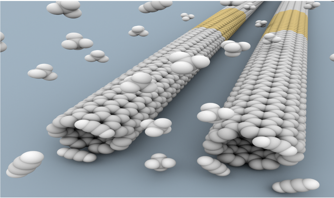
Wafer-Scale Aligned Carbon Nanotubes Synthesis
In order to demonstrate truly integrated nanotube circuits and wafer-scale fabrication, technological components such as wafer-scale synthesis and transfer of aligned nanotubes, and integrated submicron-scale device fabrication and tuning, are highly desired for the high-performance integrated nanotube circuits. Aligned nanotube growth was previously limited to small pieces of quartz or sapphire substrates. Recently, we successfully synthesized aligned SWNTs arrays on 4 inch quartz and sapphire wafers.

(a) Photograph of 4 inch sapphire wafer with aligned nanotubes. (b) Schematic diagram of 9 feet-long furnace for wafer-scale nanotube growth. (c) and (d) SEM images of aligned nanotubes and Temperature flow charts for the annealing and the nanotube growth on sapphire and quartz wafer, respectively.
Separated Carbon Nanotubes
To address the problem of coexistance of metallic and semiconducting nanotubes, nanotubes pre-separated using density gradient ultracentrifugation can be used. This gives predominently semiconducting nanotubes with purity up to 99%. We have demonstrated ways to deposit uniform separated semiconducting nanotube thin-films and further demonstrated high-performance thin-film transistors and display electronics. Compared with other channel material for thin-film transistors such as amorphous silicon or organic materials, the solution processed separated nanotube thin-films have the advantages of room-temperature processing compatibility, transparency, flexibility, and extraordinary mobility. This platform can also be used in applications such as flexible/transpratent electronics, display electronics, and printed electronics.

Wafer-scale Integrated Circuits based on Aligned Nanotubes
The device fabrication based on transferred nanotubes on 4 inch Si/SiO2 wafer was obtained by standard silicon CMOS technology such as projection photolithography using a stepper with 0.5 mm resolution for submicron device patterning, metal deposition for electrodes, and high k dielectric (HfO2 or Al2O3) deposition for gate dielectric. In addition, chemical doping has been used to build fully integrated complementary inverter with a gain ~ 5, and a defect-tolerant design has been employed for NAND and NOR gates.

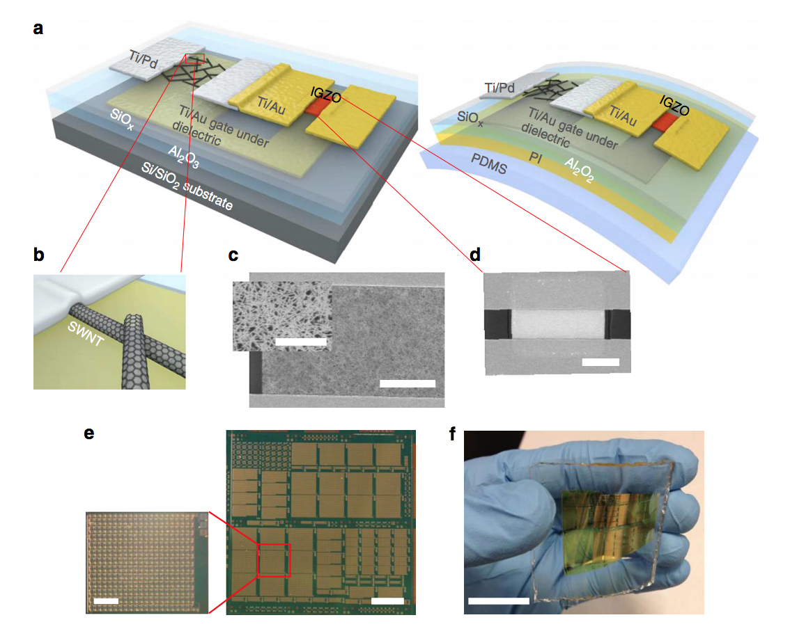
Photo images of nanotube devices and circuits built on a 4 inch Si/SiO2 wafer: 1. Back-gated transistor, 2. Top-gated transistor, 3. RF transistor, 4. CMOS inverter, 5. NOR logic gate, 6. NAND logic gate, and 7. Ring oscillator.
Surface Aligned Nanotubes
Transistor studies
Based on the aligned nanotube arrays on insulator, we studied the transistors with various device structures such as top-gated devices, polymer gated devices. Efforts have also been put to transfer the nanotube arrays to other surfaces, for example, flexible polyimide substrates.
Growth of Carbon Nanotubes at Desired Sites
CNTFET fabrication is a mature technique in our group. With our superior fabrication approach, which allows high quality individual SWCNT to be grown at desired sites and easily integrated into complicated circuits, a series of novel nanotube devices have been realized and evaluated.
Transistors
This technique shown above has led us to demonstrate p type single-walled nanotube transistors that “mimic” silicon based metal-oxide-semiconductor field effect transistors (MOSFET).
Inverters
To move one-step forward toward CNT – based integrated circuits, we have also successfully demonstrated nanotube complementary inverters in our previous work. N-type CNTFETs were obtained by doping nanotubes with potassium vapor and then integrated with p-type CNTFETs to construct complimentary field-effect inverters.
Partially Exposed Devices
To control the performance of a carbon nanotube FET, we demonstrated an approach to engineer the band structure of carbon nanotube field-effect transistors via selected area chemical gating. By exposing the center part or the contacts of nanotube devices to oxidizing or reducing gases, a good control over the threshold voltage and subthreshold swing has been achieved.
Related Publications:
1. “CMOS-Analogous Wafer-Scale Nanotube-on-Insulator Approach for Submicrometer Devices and Integrated Circuits Using Aligned Nanotubes”,
K. Ryu, A. Badmaev, C. Wang, A. Lin, N. Patil, L. Gomez, A. Kumar, S. Mitra, H. Wong, C. Zhou
Nano Letters, 9, 189 (2009). (PDF)
2. “Device study, chemical doping, and logic circuits based on transferred aligned single-walled carbon nanotubes”,
C. Wang, K. Ryu, A. Badmaev, N. Patil, A. Lin, S. Mitra, H.-S. P. Wong and C. Zhou,
Applied Physics Letters, 93, 033101 (2008). (PDF)
3. “Diameter dependence of aligned growth of carbon nanotubes on a-plane sapphire substrate”
X. Liu, K. Ryu, S. Hang, A. Badmaev, and C. Zhou,
Journal of Physical Chemistry C 112, 15929-15933. (2008) (PDF)
4. “Synthesis of Aligned Single-Walled Carbon Nanotubes Using Catalysts Defined by Nanosphere Lithography”,
K. Ryu, A. Badmaev, L. Gomez, F. Ishikawa, B. Lei, and C. Zhou
J. of Am. Chem. Soc. 129, 10104 – 10105 (2007). (PDF)
5. “A Novel Nanotube-on-Insulator (NOI) Approach toward Nanotube Devices”,
X. Liu, S. Han, and C. Zhou
Nano Letters, 6, 34-39 (2006). (PDF)
Reported by Scientific American:
http://www.sciam.com/article.cfm?chanID=sa006&articleID=0003D2B9-2FD1-1417-AE6E83414B7F0000&colID=5
6. “Template-Free Directional Growth of Single-Walled Carbon Nanotubes on a- and r-Plane Sapphire”,
S. Han, X. Liu, and C. Zhou,
J. of Am. Chem. Soc. 127, 5294 – 5295 (2005). (PDF)
Reported by USC, Materials Today, and many online publishers.
7. “Synthesis and Electronic Properties of Individual Carbon Nanotube / Polypyrrole Nanocables”,
X. Liu, J. Ly, S. Han, D. Zhang, M. Thompson, and C. Zhou,
Advanced Materials 17, 2727-2732 (2005). (PDF)
8. “Band Engineering of Carbon Nanotube Field-Effect Transistors via Selected Area Chemical Gating”,
X. Liu, Z. Luo, S. Han, T. Tang, D. Zhang, and C. Zhou,
Appl. Phys. Lett. 86, 243501 – 1-3 (2005). (PDF)
9. ”Giant Random Telegraph Signals in the Carbon Nanotubes as a Single defect Probe”,
F. Liu, M. Bao, H. Kim, K. L. Wang, C. Li, X. Liu, and C. Zhou,
Appl. Phys. Lett. 86, 163102 – 1-3 (2005). (PDF)
10. “Determination of the Small Band Gap of Carbon Nanotubes Using the Ambipolar Random Telegraph Signal”,
F. Liu, M. Bao, K. L. Wang, X. Liu, C. Li, and C. Zhou,
Nano Letters 5, 1333 – 1336 (2005). (PDF)
11. “Nanosignal Processing: Stochastic Resonance in Carbon Nanotubes That Detect Subthreshold Signals”,
Y. Lee, X. Liu, B. Kosko, and C. Zhou,
Nano Letters 3, 1683 (2003). (PDF)
12. “Carbon Nanotube Field-Effect Inverters”,
X. Liu, R. Lee, J. Han, C. Zhou
Appl. Phys. Lett. 79, 3329 (2001). (PDF)
13. “Modulated Chemical Doping of Individual Carbon Nanotubes”,
C. Zhou, J. Kong, E. Yenilmez, H. Dai
Science 290, 1552 (2000). (PDF)
14. “Potassium Doped Semiconducting Carbon Nanotubes as Single Electron Transistors”,
J. Kong, C. Zhou, E. Yenilmez, H. Dai
Appl. Phys. Lett. 77, 3977 (2000). (PDF)
15. “Intrinsic Electric Properties of Individual Single-Walled Carbon Nanotubes with Small Band Gaps”,
C. Zhou, J. Kong and H. Dai
Phys. Rev. Lett. 84, 5604 (2000). (PDF)
16. “Reversible Electromechanical Characteristics of Carbon Nanotubes under Local Probe Manipulation”,
T.W. Tombler, C. Zhou, L. Alexseyev, J. Kong, H. Dai, L. Liu, C.S. Jayanthi, M. Tang, S. Wu
Nature 405, 769 (2000). (PDF)
17. “Controllable reversibility of an sp2 to sp3 transition of a single wall nanotube under the manipulation of an AFM tip: A nanoscale electromechanical switch?”
L. Liu, C.S. Jayanthi, M.J. Tang, S.Y. Wu, T.W. Tombler, C. Zhou, L. Alexseyev, J. Kong, H. Dai
Phys. Rev. Lett. 84, 4950 (2000). (PDF)
18. “Transport Measurements of Individual Semiconducting Singled-Walled Carbon Nanotubes of Various Diameters”,
C. Zhou, J. Kong and H. Dai
Appl. Phys. Lett. 76, 1597 (2000). (PDF)
19. “Gating Individual nanotubes and Crosses with Scanning Probes”,
T.W. Tombler, C. Zhou, J. Kong, H. Dai
Appl. Phys. Lett. 76, 2412 (2000). (PDF)
20. “Nanotube Molecular Wires as Chemical Sensors”,
J. Kong, N. Franklin, C. Zhou, S. Peng, K. Cho, H. Dai
Science 287, 622 (2000). (PDF)
21. “Controlled Chemical Routes to Nanotube Architectures, Physics and Devices”,
H. Dai, J. Kong, C. Zhou, N. Franklin, T. Tombler, A. Cassell, S. Fan, M. Chapline
J. of Phys. Chem. B 103, 11246 (1999). (PDF)
22. “Synthesis, Integration and Electrical Properties of Individual Single-Walled Carbon Nanotubes”,
J. Kong, C. Zhou, A. Morpurgo, H.T. Soh, C.F. Quate, C. Marcus, H. Dai
Appl. Phys. A 69, 305 (1999). (PDF)